Category: Electronics

  • Electronic Load – Proof of Concept

    Electronic Load – Proof of Concept

    An electronic load is a piece of lab test equipment that is used to observe the behavior of devices under test (DUTs) under electric load, i.e. how they behave when we draw power from them. Electronic loads achieve this by dissipating an adjustable amount of power in their circuits, such that either a constant current or a constant power is drawn from the DUT. Most of the commercially available electronic loads can do more than that and can even be configured to perform automatic tests on devices and log the results; this is why electronic loads are also known as programmable loads.

    I need an electronic load to test my power electronics designs for battery and solar projects, and as a hobbyist I don’t want to spend much money on such a specific piece of kit. Besides, it is a great opportunity to learn about power electronics and the construction of precise equipment.

    This project is separated into different stages. For now we’ll focus on the constant current mode of the electronic load and get a feel for the basic circuit, a proof of concept, so to speak. We’ll add more advanced features in subsequent posts.

    Voltage to Current Converter

    The basic building block of most electronic loads, including ours, is the voltage to current converter. This is a circuit that takes a voltage as an input and regulates a current to change according to the input voltage. For example, in the case of the constant current operation of our electronic load for each volt of input voltage at the voltage to current converter one ampere of current flows through the electronic load. The input voltage comes from a potentiometer, so with the turn of a knob we can adjust how much current we want to draw from the DUT.

    Voltage to Current Converter Using an Operational Amplifier
    Voltage to current converter realized with an operational amplifier.

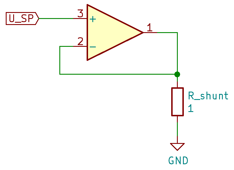
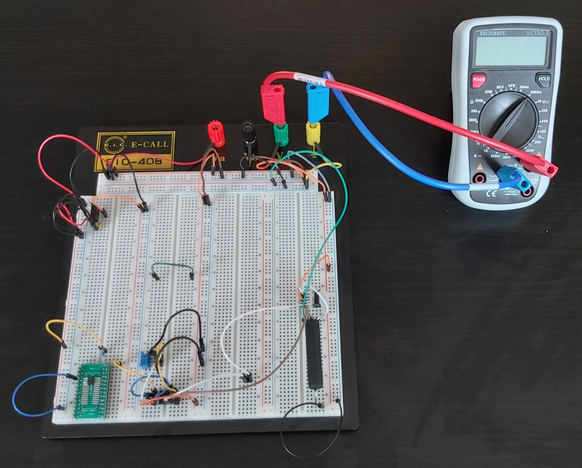
    One way to realize a voltage to current converter is with an operational amplifier (OP), see schematic. In this circuit a current I_\mathrm{L}, the load current, flows through the resistor R_\mathrm{shunt}. According to Ohm’s law, this current causes a voltage V_\mathrm{shunt}=R_\mathrm{shunt}I_\mathrm{L} between the ports of R_\mathrm{shunt}. Thus, with the knowledge of the resistance R_\mathrm{shunt}, we know can tell the current I_\mathrm{L} by measuring the voltage V_\mathrm{shunt}. This is also the cause for the name we have given the resistor; resistors that are used to measure currents via the voltage drop across them are called shunts. In the example schematic and our final design we have a shunt resistance of 1\,\Omega, that means for every ampere of load current we measure one volt of shunt voltage.

    The regulation of the current happens in the OP that compares the shuntvoltage V_\mathrm{shunt} at its inverting input to the setpoint voltage V_\mathrm{SP} at its positive input, and regulates its output voltage to a value that matches the two input voltages. This description is pretty simplified but I don’t want to go into the details of OPs in this article.

    Great, now we have a circuit, that lets us control a current by adjusting a voltage. But where is this current coming from? It is sourced by the OP, not by the DUT. We could use the DUT to power the OP, thus, all the current the OP sources would come from the DUT. This has a number of disadvantages, though; the power consumption of the OP itself is added to the power draw off the DUT, but not measured at the shunt, we limit the design by the supply voltage requirements of the OP and most importantly, standard OPs can only source small amounts of current, up to 40\,\mathrm{mA} in the case of the LM358 I’m using. How can we circumvent this problem? For this design, we will use the OP to control the gate of a power MOSFET rather than sourcing the current directly.

    MOSFET Shunt Network

    Voltage to Current Converter Using an Operational Amplifier and Transistor.

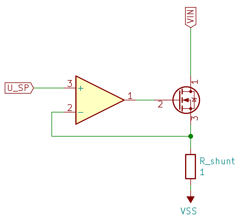
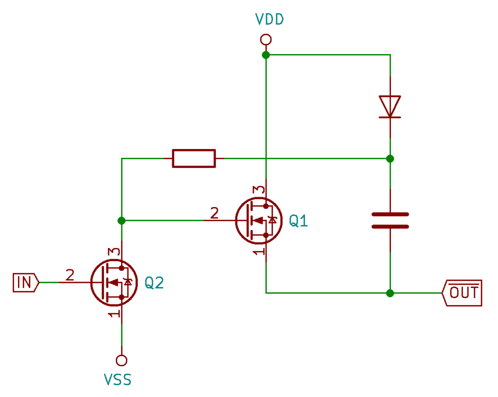
    To build a voltage to current converter with a MOSFET, we need the current to pass through the drain-to-source path in the MOSFET and a voltage controlling the current at the gate. As you can see in the schematic on the left, we connected the negative terminal of the shunt resistor the the negative supply voltage of our circuit V_\mathrm{SS}. This means that V_\mathrm{SS} will be shorted to the negative input from the DUT.

    The way this new circuit works is similar to the version without the MOSFET. The OP is input the shunt voltage V_\mathrm{shunt} and the setpoint voltage V_\mathrm{SP} and adjusts its output, such that the shunt voltage becomes equal to the setpoint voltage. In the version without the OP this means that the output voltage takes a value that caused the desired current in the shunt resistor, according to ohms law, but in the version with MOSFET it will cause the OP to output a value that causes the MOSFET to be just conductive enough to get the desired current value.

    Ok, now that we can draw a desired and potentially big amount of current / power from the DUT, we should ask ourself an important question: Where is the energy going? In electronics, we have power losses at a component, whenever there is current and a voltage drop across the component at the same time. The power this component then dissipates in the form of heat is given by P=UI\ , with U being the voltage.

    In our circuit the current comes from the DUT, flows through the MOSFET and the shunt resistor and then returns to the DUT, so we have energy dissipation at these two components. The power dissipated is given by the current and the resistace, since using Ohm’s law, we can represent the voltage drop across the resistor V_\mathrm{shunt} by the current I and the shunt resistance R_\mathrm{shunt}:P_\mathrm{shunt}=R_\mathrm{shunt}I^2\ . For the MOSFET the power dissipation is given by the product of the DUT current I and the voltage drop across the drain to source P_\mathrm{MOSFET}=(V_\mathrm{IN} – V_\mathrm{shunt})I\ . Since V_\mathrm{IN} is always greater than V_\mathrm{shunt} (otherwise there would be no current), the majority of the power is dissipated in the MOSFET.

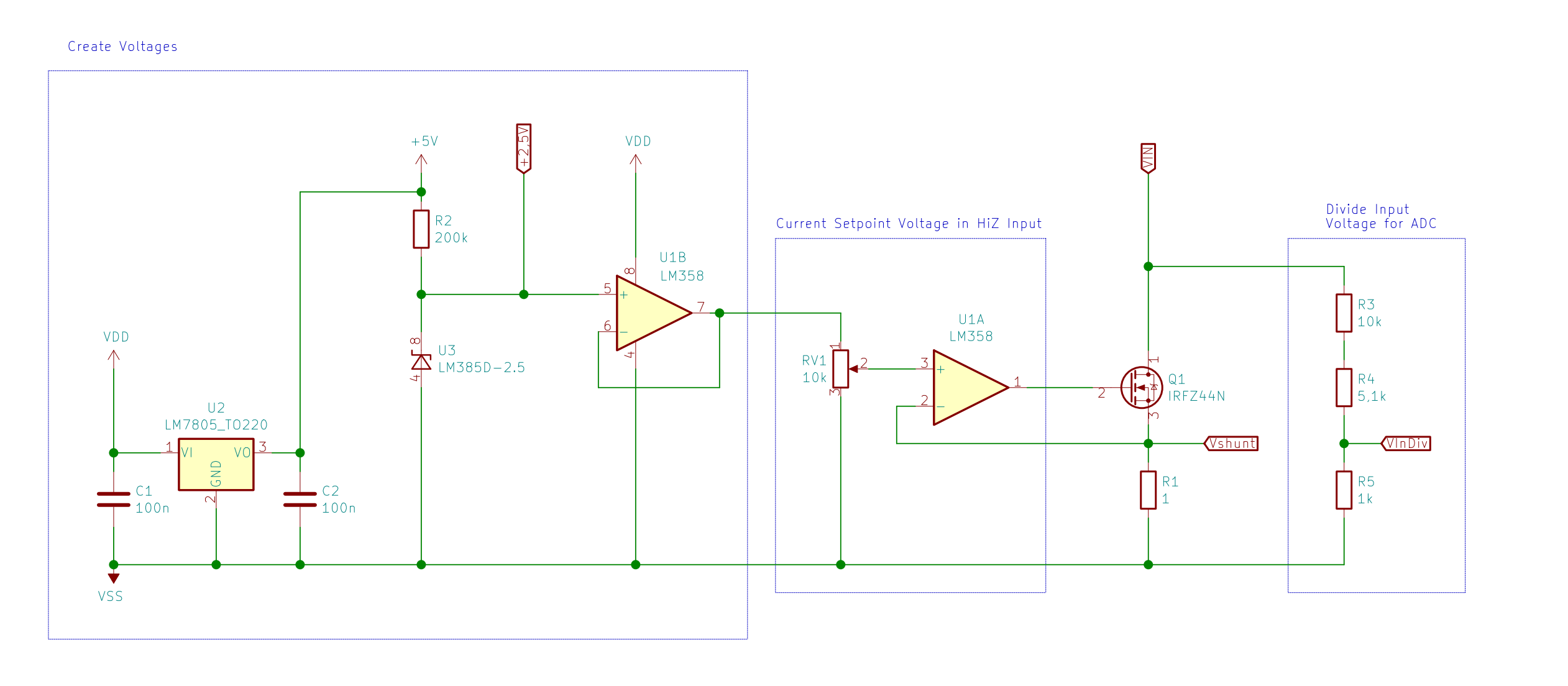
    We now have to pick components that can handle this much power disspiation, but to know which exact power rating we are looking for, we first have to ask ourselves what kind of inputs we want to feed into the electronic load. I would like it to be able to take input voltages up to 30\, \mathrm{V}, since this will allow me to characterize 7s LiPo batteries and I think 2\, \mathrm{A} should be plenty for now. I want to keep V_\mathrm{shunt} under 3.3\,\mathrm{V}, so I’m able to measure it with the integrated ADCs of some microcontrollers in the future and I also have a 2.5\,\mathrm{V} voltage reference that I can use, so with R_\mathrm{shunt}=1\,\mathrm{\Omega} the electronic load can take currents up to 2.5\,\mathrm{A}.

    At 30\,\mathrm{V} and 2.5\,\mathrm{A} input we dissipate P_\mathrm{shunt}=6.25\,\mathrm{W} in the shunt and P_\mathrm{MOSFET}=68.75\,\mathrm{W}. For the shunt this means, we will be fine with a resistor rated for 10\,\mathrm{W}; this results in a maximum current of 3,16\,\mathrm{A}. For the MOSFET it would be nice to use a jelly bean part like the IRFZ44N. This transistor is rated for 94\,\mathrm{W}, so it will do just fine, and with its breakdown voltage of 55\,\mathrm{V} we can even take inputs up to 36\,\mathrm{V} at 2.5\,\mathrm{A} and be well within its power rating.

    So, to summarize, our electronic load will have the following input ranges:

    • Input voltage: 0 – 36\,\mathrm{V}
    • Input current: 0 – 2.5\,\mathrm{A}

    Final Schematic

    With the above considerations I end up with this Schematic, however, I added a voltage divider on the right, that maps the input voltage in the range of 0-2.5\,\mathrm{V} to be able to use that as well in future versions of the circuit.

    Schematic of my Proof-of-Concept Electronic Load
    Breadboard Assembly of my Proof-of-Concept Electronic Load
    Design of this stage on a breadboard. Adjusting the setpoint for the shunt voltage is done with a trimmer poti and the monitoring of the shunt voltage happens with an external multimeter.

    Outlook

    We successfully created a working proof of concept for an electronic load. It may be simple and not much to look at yet, but we can already test the behavior of DUTs loaded with a constant current.

    Of course, I actually plan to use my electronic load in my lab and for this there still is a lot to do:

    • Safety features that protect the circuit from overcurrent, overvoltage, overpower and overheating
    • Moitoring and setpoint adjustment as part of the EL
    • A case with a nice display, a knob and banana janes for the DUT

    So stay tuned for updates!

  • Voltage Multiplier / Charge Pump

    Voltage Multiplier / Charge Pump

    In this article I will show you how I designed my voltage multiplier board, consisting of the actual multiplier circuit, the driver for the multiplier and an oscillator.

    Voltage Multiplier Circuit

    Working Principle of a Cockcroft-Walton Multiplier
    Working principle of a Cockcroft-Walton Multiplier. The two lower diagrams show the two states of the signal.

    This circuit takes low input voltages like 5 V or 12 V and generates high voltages from it. For a 12 V input it generates over 100 V of output voltage, albeit with very low power. It is based on the Cockcroft-Walton Multiplier or Greinacher Multiplier, a simple circuit that has been used since the 1930s to generate high voltages, originally for particle accelerators. It uses the nonlinear properties of diodes to change the voltage reference of a charged capacitor. A simple 2-stage multiplier is shown on the right. The capacitors are connected to the intermediate stages on the one side and to a signal and its inverse on the other. This signal switches between the input voltage VDD and GND.

    For continous operation let’s assume both capacitors are charged with a voltage of VDD. In state 1 the signal is at VDD and its inverse is at GND. Since the capacitor at stage one is charged, the potential at its upper side is 2x VDD. The input diode is not conducting and the capacitor of the second stage is charged by the capacitor of the first stage until both of them are charged to almost 2x VDD (ignoring the voltage drop of the diode). In state 2 the first capacitor is recharged through the input diode, while the second capacitor has a potential of VDD at its lower side and is still charged with a voltage of 2x VDD. Thus, the potential at the second stage is now almost 3x VDD. Each stage adds approximately the value of the input voltage to the output voltage. By using a larger number of stages high voltages can be achieved. Note that all current flowing out of the output was flowing in through the input diode and moved by altering the signal; in this sense this circuit can be considered a charge pump.

    Oscillator

    Astable Multivibrator Oscillator Circuit
    Multivibrator circuit used to generate the signals for the voltage multiplier.

    To drive this voltage multiplier we need the two signals. For this we can use a simple multivibrator circuit like it is shown on the left. This is a well known basic circuit, so I won’t go into much detail here. The values of the passive components make the multivibrator oscillate at around 1 kHz.

    Driver Circuit

    The outputs of oscillator circuits can be rather delicate and the signals are supposed to charge the capacitors of the output stage fast, so rather than using the outputs of the multivibrator directly I will buffer then with a bridge circuit made from power MOSFETs.

    CMOS Half-Bridge
    Ordinary MOSFET bridge circuit with a n-channel MOSFET on the low side and a p-channel MOSFET on the high side.

    Your usual MOSFET bridge looks like the circuit on the right; the output is connected to the supply rails through a n-channel MOSFET on the low side and a p-channel MOSFET on the high side. Since the threshold voltage acts differently on the n- and p-channel MOSFETs we can even use the naked signal to drive both MOSFETs at once. Although this circuit is nice and simple it has a few disadvantages: p-channel MOSFETs tend to have a higher on resistance than their complementary n-channel counterparts and they are also usually more expensive. Most importantly, though, I didn’t have any lying around, so I’m doing something a bit more fancy: I’m bootstrapping an n-channel MOSFET to use it on the high side.

    High Side N-Channel Switches

    If you want to use an n-channel MOSFET on the high side you’ll quickly notice a problem: If you want to switch the MOSFET on, you have to pull the gate above the threshold voltage. However, as soon as the MOSFET is on, the source is effectively at the rail voltage VDD and the voltage difference between the gate and the source becomes zero. So, to maintain its on-state the MOSFETs gate has to be above the rail voltage. Sure you could just design your power supply to deliver a such voltage, but this is a lot of work and also PCB space and there is a simpler solution: Bootstrapping

    High Side N-Channel MOSFET Switch
    Bootstrapped high-side n-channel MOSFET.

    Bootstrapping works on the same principle as the voltage multiplier circuit. It uses diodes to move a charged capacitor to a higher potential. The circuit for bootstrapping a high-side n-channel MOSFET can be seen on the left. If the input signal is low, i.e. Q2 is off, the supply rail charges the small capacitor and Q1’s gate. As soon as Q1’s gate surpasses the threshold voltage Q1 switches on and the lower side of the capacitor is at the supply voltage VDD. Its upper side is now above the supply voltage and keeps this voltage, because the diode is not conducting. The upper side of the capacitor is connected to Q1’s gate, so Q1 remains switched on. If the input signal goes high, Q1’s gate and the capacitor are discharged through Q2 and Q1 switches off.

    There are some things to keep in mind with this technique. Since capacitors don’t stay charged forever due to leakage you can’t use this for stationary switching, but only for changing input signals. Another thing to keep in mind is to not choose the value of the capacitor too high or too low. If it is too high, the capacitor charges too slow compared to the gate of Q1 and the bootstrapped voltage will not be high enough. If it is too low, the bootstrapped voltage will be more vulnerable to leakage. A choice that works for me and my IRFZ44N MOSFETs with about 1.5 nF gate capacitance is to pick a 1 kΩ resistor and a 10 nF capacitor.

    Furtheremore, note that all Q2 does is discharging Q1’s gate and the external capacitor so it doesn’t have to be a power MOSFET. I went with 2N7000 small-signal MOSFETs.

    Bootstrapped MOSFET Bridge

    A Pure N-Channel Transistor Bridge Using Bootstrapping on the High Side
    Bootstrapped n-channel MOSFET bridge.

    With the bootstrapped n-channel high-side MOSFET my final bridge circuit looks like this. It is a high-side n-channel MOSFET, combined with a simple low-side n-channel MOSFET and a pull-down resistor to keep the output at a well-defined potential during switching. Without the pull-down resistor Q1’s gate would be floating at a low input signal.

    This driver generates nice and stable signals to drive the multiplier circuit.

    Result

    My final schematic looks like this:

    Schematic of my Voltage Multiplier Board
    Final schematic of my voltage multiplier.

    To put a lid on this project and refine my PCB skills, I designed one for it and had it manufactured. With 5 V input voltage to the multivibrator and 12 V input voltage to the driver circuit I actually see an output voltage of over 100 V.

    Operation of the final circuit. The output voltage reaches over 100 V, but the oscillator waveform is not optimal.

    But this circuit is not perfect. There are a few things I want to point out:

    • The output waveforms of the multivibrator look terrible.
    • The IRFZ44N MOSFETs are propably too beefy for this job; I only chose them because they had the lowest on-resistance of all the MOSFETs I had at home.
    • The operating frequency and the capacitor values in the voltage multiplier work, but they are not calculated to deliver some sort of optimum. They are more like educated guesses.

    Despite these things I may revisit in the future, it was a fun and successful project in which I learned a lot!